Module electronics
SunSolve Yield models the full electrical behaviour of photovoltaic modules using a physically based circuit approach. Each solar cell is represented by a one-diode equivalent circuit, connected in a network that replicates the module’s true electrical layout — including series and parallel strings, interconnects, and optional bypass diodes. The light-generated current for every cell is directly derived from the ray-traced optical absorption, while temperature-dependent electrical parameters are solved at each time step to determine current–voltage (IV) characteristics and module output. This approach provides a consistent, physics-based link between optical, thermal, and electrical domains within the simulation.
The table below provides a summary of the module electronics models.
| Parameter | Model | Notes | Reference |
|---|---|---|---|
| Cell current-voltage output characteristics | 1-diode equivalent circuit with Rs and Rp | The de facto standard in the PV industry. See the references for a comprehensive review. | [Chin2015] [McIntosh2001] |
| Irradiation dependent shunt resistance | PVsyst irradiation dependent shunt model | Mainly this is intended for non-crystalline silicon devices. | [Mermoud2013] [Mermoud2014] |
| Module circuit | DC SPICE circuit | A full SPICE model of module is defined and solved. | [SPICE3f5] |
| Diode model | Level 1 SPICE model | Based on the SPICE 3f5 implementation from Berkley University | [SPICE3f5] |
| Calculation of cell series resistance | Set of analytical equations | Only applies to complex modules. | [Green1982] |
| Temperature dependence of current-voltage output | PVsyst model | [Mermoud2014] |
Equivalent circuit model of solar cell
Section titled “Equivalent circuit model of solar cell”The equivalent circuit model for the solar cell is shown in the figure below. It includes a current source for the light generated current, a single diode for the recombination within the device and shunt and series resistors for the electrical loss of majority carriers. This circuit is widely used in yield modelling to calculate the electrical output of cells and modules under a wide range of operating conditions.
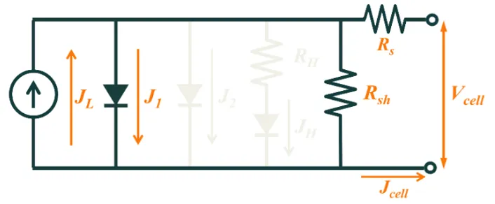 Equivalent circuit of solar cell.
Note that in SunSolve Yield the n=2 diode and resistive limited enhanced recombination components are disabled. This is necessary as the currently applied temperature model does not account for them and for many PV modules the full set of measured outputs required to determine these inputs are not known.1
The IV characteristics are determined using the following equations:
Where I0 , n, Rs, and Rsh are the circuit inputs for saturation current, ideality factor, series resistance and shunt resistance; all defined at a nominal temperature (typically 25°C). IL is the light generated current which is linked to the result of the ray tracing.
Optionally an irradiation dependent shunt resistor may be defined. This model is more applicable to non-crystalline silicon devices and in modern high efficiency modules can likely be neglected in most cases. Note that it is unclear how the inclusion of this model impacts the reverse bias behaviour if included simply to match the low light behaviour of the max power point.
Where G is the irradiance, Gref is the reference irradiance (typically 1000 W/m2), Rsh,0 is the shunt resistance at zero irradiance, Rsh,ref is the shunt resistance at the reference irradiance and Rsh,exp is the exponent (typically 5.5 for c-Si and >10 for other technology).
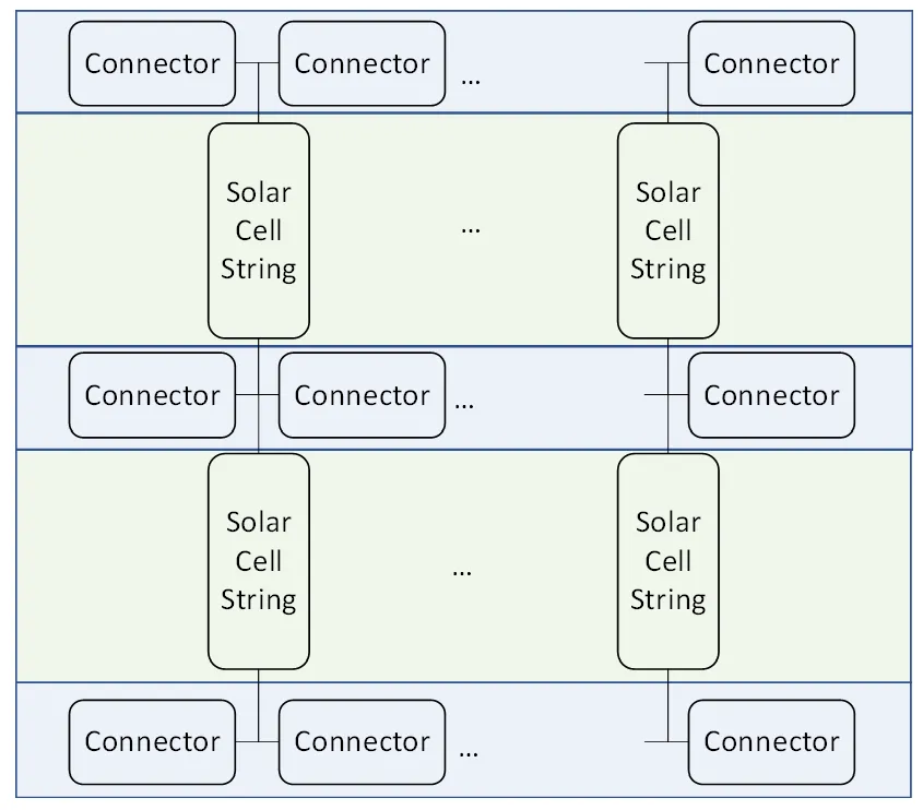
Module circuit
Section titled “Module circuit”The module circuit comprises an array of ‘connectors’ and ‘cell strings’ joined via a matrix of node points (see figures below).
The connectors define how cell strings are joined together and may be one of four types:
-
Open-circuit: no current will flow through the connector and the nodes on either side are electrically isolated.
-
Short-circuit: a lossless connection (i.e. resistance = 0 Ω) through which current may flow between adjacent nodes.
-
Bypass diode: a single SPICE diode as described below, the diode may face either direction.
-
Module terminal: the end points of the module circuit that connect it to the external load, each panel must have one positive and one negative terminal.
A cell string contains one or more solar cell equivalent circuits connected from positive terminal to negative terminal. The cells may be arranged such that under illumination the current flows in either direction through the string.
There are three different circuit layouts implemented:
-
Traditional c-Si: alternating rows of ‘connectors’ and ‘cell strings’. This model can be configured to match a wide variety of c-Si PV modules.
-
Odd columns with return path: an odd number of cell string columns with an extra column that contains a return path (implemented as a short circuit). This is used to model panels with the larger half-cut cell size.
-
Horizontal string: two columns of ‘connectors’ with a single column of parallel ‘cell strings’ in the middle. This layout is more commonly used by thin film modules such as the FirstSolar CdTe products.
The traditional c-Si layout is shown below it comprises of alternating rows of connectors and cell strings. A minimum of one cell string with four connectors is required. More cell strings can be added in both the X and Y directions. For each new column added a new set of connectors is added to each row. Note that many of the outer connectors are typically set to open-circuit.
 Generic circuit layout for the ‘Traditional c-Si’ option. Matrix comprises of
alternating rows of connectors and cell strings.
Generic circuit layout for the ‘Traditional c-Si’ option. Matrix comprises of
alternating rows of connectors and cell strings.
Two examples of traditional c-Si module circuits are shown below. Both feature sets of parallel strings of cells connected with three bypass diodes.
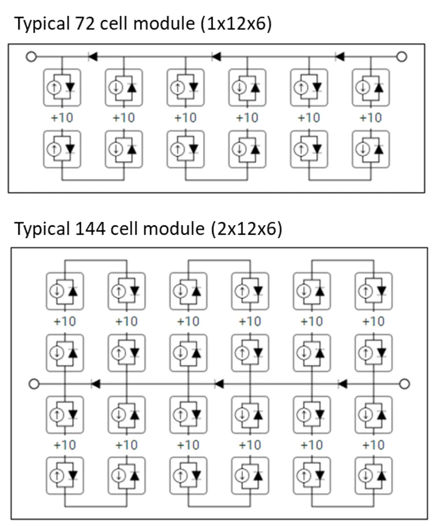 Example module circuits for the ‘Traditional c-Si’ option.
The horizontal strings layout is shown below, it comprises of two columns of connectors and a middle column of parallel cell strings. A minimum of one string with a pair of connectors (module terminals) is required. New parallel cell strings with a pair of connectors (short circuit) may be added as new rows.
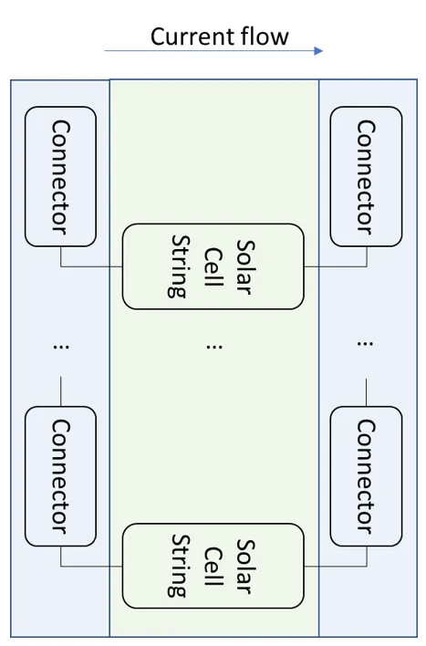 Generic circuit layout for the ‘Horizontal strings’ option. Matrix comprises of
two columns of connectors and a middle column of parallel cell strings.
Generic circuit layout for the ‘Horizontal strings’ option. Matrix comprises of
two columns of connectors and a middle column of parallel cell strings.
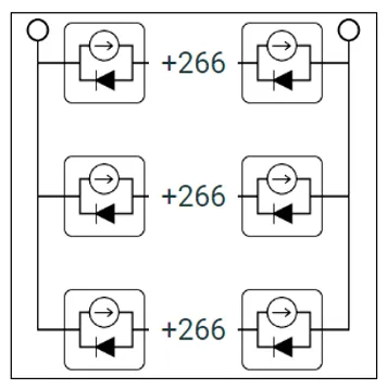 Example module circuits for the ‘Horizontal strings’ option. In this case there
are three parallel strings each with 268 cells in series.
Example module circuits for the ‘Horizontal strings’ option. In this case there
are three parallel strings each with 268 cells in series.
Bypass diode model
Section titled “Bypass diode model”There are two models available for the bypass diodes, both are based on the common SPICE approach for the modelling of diodes.
The ‘Simple’ model has no temperature dependence, no series resistance and no reverse breakdown. The current through the bypass diode (IB) is determined from:
Where IS,B is the saturation current and NB is the diode ideality factor.
The ‘SPICE Level 1’ model enables the definition of RS,B which is an Ohmic resistor in series with the diode. It also enables the definition of a ‘knee-on’ reverse bias breakdown voltage BV at which point the diode current transitions towards flowing reverse bias breakdown ‘knee’ current IBV. Temperature dependence of the saturation current is achieved through the definition of a bandgap voltage (EG) and a temperature exponent XTI as shown in the follow equation:
Note that bypass diodes in solar modules do not typically have reverse breakdown behaviour within the range of reverse voltage they would typically experience, and as such the value of BV can be set very high.
The figure below demonstrates the fitting of the diode model to a typical solar bypass diode.
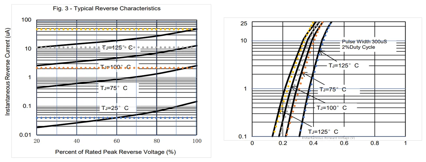 Comparison between the simulation of a typical solar bypass diode with the full
SPICE level 1 model (symbols) and the forward (right) and reverse (left) diode characteristics as reported on a
datasheet (lines).
Comparison between the simulation of a typical solar bypass diode with the full
SPICE level 1 model (symbols) and the forward (right) and reverse (left) diode characteristics as reported on a
datasheet (lines).
Determination of cell light generated current
Section titled “Determination of cell light generated current”The light generated current within each cell is calculated at every time step using the following procedure:
-
The wavelength dependent photon count for the direct and isotropic components of incident irradiance are adjusted based on the selected sky model.
-
The wavelength dependent absorption within the cell is calculated for the specific sun position based on the linear interpolation of the nearest three solar angles.
-
At each wavelength the four components of light generated current are calculated as:
Where SF is the wavelength dependent scaling factor that is applied to simple modules based on their quantum efficiency and STC value of front and rear ISC (as described in Module current scaling). For complex modules this is not required.
-
The final value for the light generated current at the nominal temperature (i.e., 25 °C) is the sum of the above four components.
The value is subsequently adjusted based on the module temperature as outlined below.
Determination of the series resistance
Section titled “Determination of the series resistance”The series resistance of each cell within the module can be set to a fixed value (no voltage or temperature dependence) by the user. Optionally, for complex modules the value can be calculated based on a set of analytical equations that accounts for:
-
The geometry of the cell, including the shape, dimensions and thickness.
-
The resistivity of the main absorbing substrate.
-
The sheet resistance between electrode fingers on the front and rear sides.
-
The contact resistance between the electrode fingers and the substrate, including calculation of the transmission length to account for the strength of the sheet resistance underneath the contact.
-
The shape, layout and resistivity of the fingers, busbars and ribbons.
-
The additional length of ribbons used to connect to the next cell.
The equations are based on the approach of calculating the power loss in the components when operating under maximum power point conditions and then converting that into a resistive value. The general approach along with many of the equations is described in the textbook by Professor Green [Green1982]. When using the analytical approach an additional amount of series resistance (Rs ,a) may be added to account for other components that are not included in the equations, such as the module connectors.
Temperature dependence of electrical circuit
Section titled “Temperature dependence of electrical circuit”The temperature dependence of the equivalent circuit inputs is determined using the PVsyst circuit temperature model [Mermoud2014]. Input values for JL, I0, and n are adjusted according to the following:
Where μL and μn are inputs to the model that represent the change in IL and n measured in %/°C and Tnominal is the specified reference temperature for IL, I0, and n (typically 25°C).
Cell-to-cell mismatch
Section titled “Cell-to-cell mismatch”SunSolve calculates the cell-to-cell mismatch at every time step of a yield simulation using the following procedure.
For each module:
-
Determine the light-generated current JL in each solar cell from the ray tracing and cell collection efficiency.
-
Determine power produced by each solar cell if they all operate at their own maximum power (solving the 1-diode model at the module temperature). The sum of those values is
-
Determine the maximum power produced by the module when all cells are connected as per the module layout, including bypass diodes in parallel with the cell strings (solving the SPICE model of the module at the module temperature). That gives PMM.
-
The absolute mismatch loss for that module is .
Then, for the unit system:
-
the absolute cell-to-cell mismatch loss is the sum of the losses for each module:
-
the relative cell-to-cell mismatch loss is
Footnotes
Section titled “Footnotes”-
The reasons for this are somewhat historical and relate to the fact that module IV outputs provided on a typical datasheet limit the number of outputs that can be measured and subsequently fitted. By including these extra circuit components there are too many input parameters that require fitting to too few outputs. This problem can be resolved with a matrix of temperature dependent IV curves and a complex curve fitting algorithm to determine the full set of inputs. Currently this is not yet implemented within SunSolve Yield. In the meantime, it is recommended to convert multiple diode circuit models into a single diode model by establishing a set of temperature and irradiation dependent operating points and then fitting to those with the single diode model. ↩