Module electronics
SunSolve Yield models the full electrical behaviour of photovoltaic modules using a physically based circuit approach. Each solar cell is represented by a one-diode equivalent circuit, connected in a network that replicates the module’s true electrical layout — including series and parallel strings, interconnects, and optional bypass diodes. The light-generated current for every cell is derived from the ray-traced optical absorption, and temperature-dependent electrical parameters are solved at each time step to determine current–voltage (IV) characteristics and module output. This approach provides a consistent link between optical, thermal, and electrical domains within the simulation.
Solar cell equivalent circuit
Section titled “Solar cell equivalent circuit”This page focuses on how SunSolve Yield connects and solves cell models at the module level (strings, interconnects, and bypass diodes). The underlying solar cell equivalent circuit model, including assumptions and governing equations, is documented separately in Equivalent circuit model.
For details of how the cell model is parameterised and updated during a yield run, see:
- Determination of cell light-generated current
- Determination of the series resistance
- Temperature dependence of electrical circuit
Module circuit
Section titled “Module circuit”The module circuit comprises an array of connectors and cell strings joined via a matrix of node points.
A cell string contains one or more solar cell equivalent circuits connected in series. The cells may be arranged such that, under illumination, the current flows in either direction through the string.
Connectors define how cell strings are joined together and may be one of four types:
- Open-circuit — no current flows; the nodes on either side are electrically isolated.
- Short-circuit — a lossless connection (resistance = 0 Ω) through which current may flow between adjacent nodes.
- Bypass diode — a single SPICE diode (see below); the diode may face either direction.
- Module terminal — the positive or negative endpoint of the module circuit that connects it to the external load.
Two circuit topologies are available:
- Vertical strings — the standard layout for crystalline silicon modules. Cells are arranged in columns, with each column divided into substrings by connector rows. Bypass diodes protect each substring. This is the default and most commonly used option.
- Horizontal strings — cells are connected in series within horizontal rows, with multiple rows connected in parallel. This layout is commonly used for thin-film modules.
The circuit topology, connector row configuration, and bypass diode parameters are configured in the Circuit tab of the module popover. See Module electrical layout for a full description of the circuit inputs.
Bypass diode model
Section titled “Bypass diode model”Each substring in the module can be protected by a bypass diode. Two SPICE-based models are available.
Simple model
Section titled “Simple model”The simple model has no temperature dependence, no series resistance, and no reverse breakdown. The current through the bypass diode () is:
where is the saturation current and is the diode ideality factor.
SPICE level 1 model
Section titled “SPICE level 1 model”The SPICE level 1 model adds a series resistance , a reverse-bias breakdown voltage (with breakdown current ), and temperature dependence via a bandgap voltage and temperature exponent :
Bypass diodes in solar modules do not typically exhibit reverse breakdown within the voltage range they experience in practice, so the value of can generally be set very high.
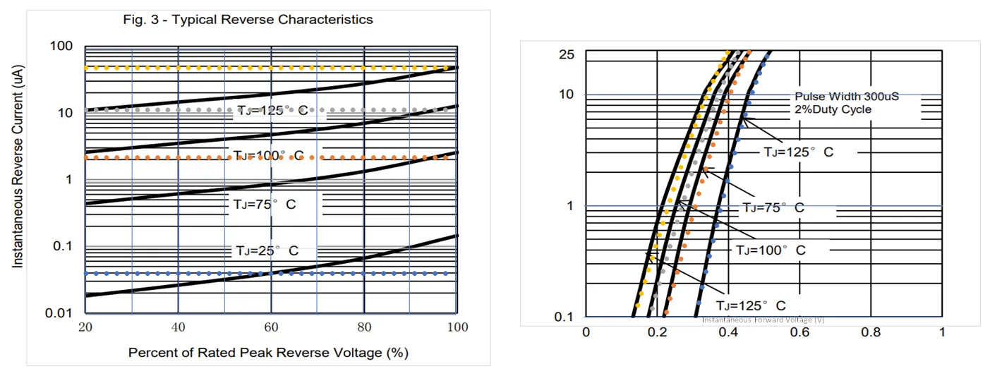 Comparison between the simulation of a typical solar bypass diode with the full
SPICE level 1 model (symbols) and the forward (right) and reverse (left) diode characteristics as reported on a
datasheet (lines).
Comparison between the simulation of a typical solar bypass diode with the full
SPICE level 1 model (symbols) and the forward (right) and reverse (left) diode characteristics as reported on a
datasheet (lines).
See Module electrical layout — bypass diodes for the input parameters of each model.
Cell-to-cell mismatch
Section titled “Cell-to-cell mismatch”SunSolve calculates the cell-to-cell mismatch at every time step of a yield simulation using the following procedure.
For each module:
-
Determine the light-generated current in each solar cell from the ray tracing and cell collection efficiency.
-
Determine the power produced by each solar cell if they all operate at their own maximum power (solving the 1-diode model at the module temperature). The sum of those values is .
-
Determine the maximum power produced by the module when all cells are connected as per the module layout, including bypass diodes in parallel with the cell strings (solving the SPICE model of the module at the module temperature). That gives .
-
The absolute mismatch loss for that module is .
Then, for the unit system:
-
The absolute cell-to-cell mismatch loss is the sum of the losses for each module: .
-
The relative cell-to-cell mismatch loss is .
Summary
Section titled “Summary”Cell IV characteristics, 1-diode equivalent circuit with and , The de facto standard in the PV industry. See Equivalent circuit model., [Chin2015] [McIntosh2001]
Irradiation-dependent shunt resistance, PVsyst model, Mainly for non-crystalline silicon devices. See Illumination-dependent shunt resistance., [Mermoud2013] [Mermoud2014]
Module circuit, DC SPICE circuit, A full SPICE model of the module is defined and solved., [SPICE3f5]
Diode model, Level 1 SPICE model, Based on the SPICE 3f5 implementation from Berkeley University., [SPICE3f5]
Cell series resistance, Analytical equations, Only applies to complex modules. See Determination of the series resistance., [Green1982]
Temperature dependence, PVsyst model, See Temperature dependence of electrical circuit., [Mermoud2014]