Cell and module layout
This section describes the 2D layout options for cells and modules.
Device configuration
Section titled “Device configuration”The highest level setting for the layout is the device configuration which is set on the Options tab.
There are four options for the device configuration:
-
Solar cell: There is no spacing between cells, irrespective of the wafer shape. The structure can have multiple layers (e.g., glass, EVA, silicon). The electrical model solves for a single solar cell.
-
Unit-cell module: The ray tracing solves a single unit cell. Spacing between cells can be included but frames cannot. If the edge condition (see below) is set to ‘100% reflectance’ then solving a unit-cell module is equivalent to solving an infinitely large module for which the optical behaviour of all cells is identical. Modifying the number of cells in the module affects the electrical behaviour but not the optical behaviour.
-
Module: A full module is simulated. Spacing between cells and frames can be included. Modifying the number of cells in the module affects both the optical and electrical behaviour. The ray tracing determines the generation current in each cell, and a SPICE circuit simulation determines the resulting electrical behaviour. This electrical solver takes into account the non-uniform generation current and hence the ‘electrical mismatch’.
-
System: A system comprised of one or more modules is simulated. See the System tab in the About section for more information on this option.
Use the ‘unit-cell module’ option if you’d like to simulate a module without frames and you’re not interested in electrical mismatch. You can then use fewer rays to determine the electrical behaviour of the module. (Electrical mismatch will be negligible for most module designs under standard illumination conditions.)
Use the ‘module’ option if you’d like to simulate a module with frames and/or you’d like to account for electrical mismatch. Be sure to simulate with a sufficient number of rays to minimise electrical mismatch due to the stochastic nature of ray tracing. E.g., increase the number of rays until the mismatch loss (provided on the ‘JV’ output tab) converges to a desired resolution.
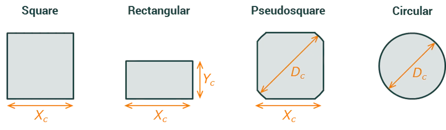
Cell dimensions
Section titled “Cell dimensions”The solar cells can either be square, rectangular, pseudosquare or circular. Their dimensions are defined in the figure below.
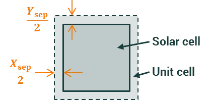
Cell spacing
Section titled “Cell spacing”A spacing can be introduced between the solar cells in the x and y directions. The figure below shows how the user inputs, and , define the distance between the edge of the solar cell and the edge of the unit cell. (The solar cell and the unit cell are concentric.)
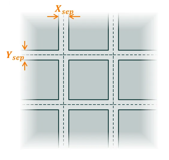
Edge condition
Section titled “Edge condition”The vertical edges of the simulation structure are assigned as being either an “ideal absorber” or an “ideal reflector”. (This input can be found on the ‘Options’ tab rather than the ‘Layout’ tab.)
When set to an “ideal absorber”, any rays that intersect the edge of the simulation are absorbed and do not return. This setting can be used to simulate a module with a single solar cell, where the light that intersects the edge of the module is lost.
When set to an “ideal reflector”, any rays that intersect the edge of the simulation are specularly reflected without any change to their intensity. This setting can be used to simulate a module with infinitely many solar cells, where the cell spacing is shown in the figure below.
Module dimensions
Section titled “Module dimensions”The figures below define the dimensions of the frame and perimeter. These inputs are only relevant when solving a module.
The layers, materials, and interfaces within the perimeter region of the module are the same as those within the cell-separation region of the unit cells. They are defined on the ‘Layers’ tab.
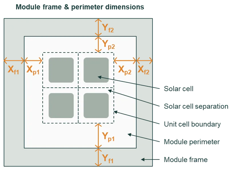
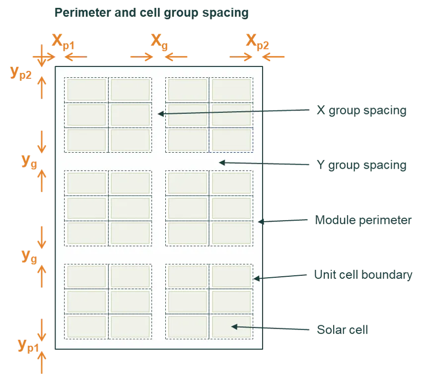
When “define cell groups” is checked, the number of cells in the columns and rows is divided into the requested number of groups. For example in the image below, the module has 4 cells in each row and 9 cells in each column, and those cells have been grouped such there are 2 cell groups in the X direction and 3 cell groups in the Y direction.
The image also shows that the distance between cell groups, and , does not add extra space to the perimeter of the module. Thus, if there were only one group in the X direction, there would be no need to define .
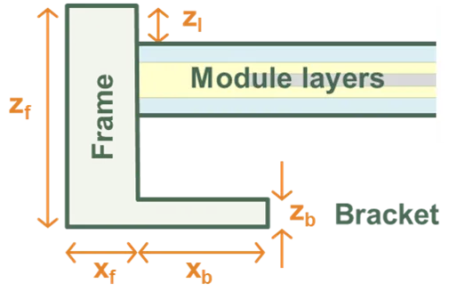
Frame and bracket geometry
Section titled “Frame and bracket geometry”The frame is defined by its width, height, and lip (overhang) dimensions, while the bracket represents the mounting structure beneath or behind the module edge. Together, they form an L-shaped cross-section around the module, as shown in the figure.
-
Frame dimensions:
Xf/Yf: horizontal thickness of the frame edgeZf: vertical height of the frame (typically 35 mm)Zl: lip height extending over the module glass
-
Bracket dimensions:
Xb/Yb: horizontal width of the bracket beneath the moduleZb: bracket thickness or vertical height
 Frame and Bracket Definition.
The frame and bracket can be configured as:
- Symmetric: identical on all four sides
- Half-symmetric: identical on two opposing sides (e.g. long edges)
- Asymmetric: fully independent dimensions for each edge
Modelling non-uniform cell behaviour
Section titled “Modelling non-uniform cell behaviour”While the cell layout defines the physical and optical arrangement of cells, modifiers can be used to model non-uniform electrical behaviour within the module. Modifiers allow you to modify equivalent-circuit parameters for specific cells or groups of cells (by row, column, or individual position), enabling modelling of partial shading, degradation, or manufacturing variations.