Main solving algorithms
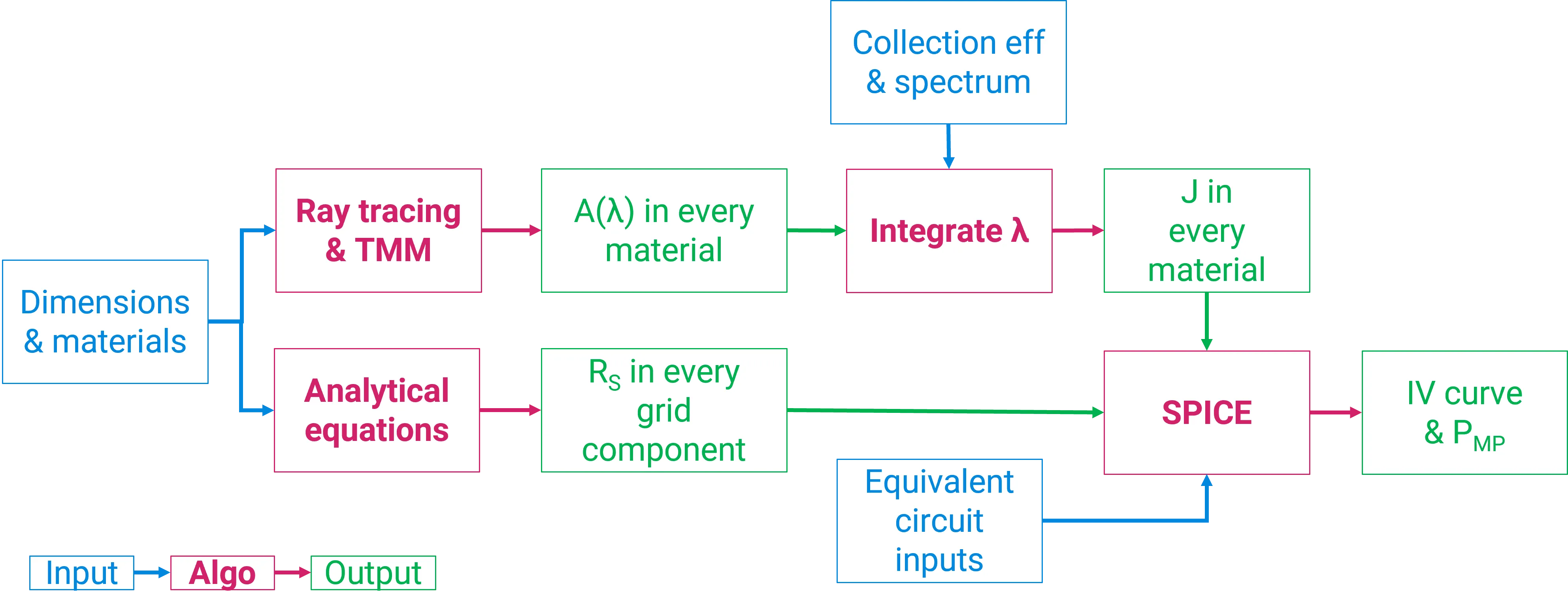
The main solving algorithm is illustrated in the figure above. The user defines all simulation inputs at the start, including device geometry, materials, illumination sources and electrical circuit parameters. SunSolve then uses ray tracing to determine optical absorption, and these optical results become inputs to the electrical model that calculates the device performance.
Basic ray tracing algorithm
Section titled “Basic ray tracing algorithm”SunSolve combines Monte Carlo ray tracing with thin‑film optics to determine wavelength‑dependent absorption, reflection and transmission throughout a device. The main solving algorithm proceeds as follows.
-
A number of rays (the value specified as Rays per packet on the Options tab) are created. Each ray is assigned a wavelength, an intensity, a direction, and a location (either above the module for front illumination or below the module for rear illumination).
-
Each ray travels in a straight line until it intersects a facet of the module surface.
-
At this interaction, and at all future interactions with an interface:
- reflectance, transmittance and absorptance are calculated. Each depends on wavelength and electric field (polarisation), as well as on the complex refractive indices of the materials on either side of the interface and any thin films between them;
- the intensity of the ray is reduced by the value of the absorptance;
- the magnitudes of reflectance and transmittance are translated into probabilities;
- a random decision, weighted by those probabilities, selects whether the ray is reflected or transmitted at the interface;
- a new direction is assigned to the ray depending on whether it is reflected or transmitted, and on the scattering model assigned to that interface;
- the ray continues through the module until it intersects another interface.
-
If the ray passes through an absorbing layer, its intensity is reduced by applying Beer’s law. This reduction in intensity is usually considered a loss (for example, absorption in the module glass), but when the ray passes through a semiconductor such as silicon, the absorption corresponds to photogeneration of electron–hole pairs and the reduction in intensity can be considered a gain.
-
Steps 2–4 are repeated for each ray until one of the following conditions is met:
- the ray is lost from the module by being reflected from the front surface or by escaping through the front or rear surfaces;
- the ray intensity decreases below a threshold defined by Intensity threshold on the Options tab; or
- the ray has intersected the maximum allowable number of interfaces, defined by Max bounces per ray on the Options tab.
-
The gains (photogeneration) and losses (reflection, transmission, parasitic absorption) are recorded for each ray, then summed and averaged to give the results for that ray packet.
-
Steps 1–6 are repeated for as many ray packets as required for the total number of rays to equal the value entered at Rays per run on the Options tab. The total gains and losses are averaged and sent to the user interface.
The global gains and losses are therefore determined by averaging a large number of rays. With a sufficiently large number of rays, the Monte Carlo simulation converges to the underlying physical model.
Electrical solving
Section titled “Electrical solving”SunSolve calculates the electrical outputs of the solar cell or module by solving an equivalent-circuit model. The solution to that model is a JV curve (i.e., the relationship between current and voltage), from which standard electrical outputs like maximum power , short-circuit current , and open-circuit voltage are determined. The electrical outputs are presented on the JV tab.
Inputs to the equivalent-circuit model are found on the Circuit tab. Most of the inputs are defined by the user but there are two possible exceptions: the series resistance (optional) and the light-collected current .
The user has two options for assigning a value to :
- Insert a value for . This option is available when electrodes have not been enabled on the Electrodes tab or when ‘Calculate grid resistance’ is not checked on the Circuit tab.
- Insert the non-grid series resistance and allow SunSolve to calculate the grid resistance . This option is available when the electrodes are enabled and ‘Calculated grid resistance’ is checked. The sum of the non-grid and grid components gives the value of used by the electrical solver.
represents the current density generated inside the solar cell and collected by the p–n junction. It’s called the light-generated current density.
is determined from this equation:
where is the incident photon current as determined from the inputs on the Illumination tab, is the fraction of the incident light that becomes absorbed by the active region of the solar cell as determined by ray tracing, and is the collection efficiency within that active region as defined on the Circuit tab.
In fact, this equation is applied for each illumination source, where light entering the front of the cell is ascribed to the front light-generated current , and light entering the rear of the cell is ascribed to the rear light-generated current . These values are summed for each illumination source to give the total used by the electrical solver.
Additional collecting layers can be defined using the Circuit tab. Each additional layer has a single collection efficiency and does not distinguish between light absorbed from the front or rear.
The Layers tab of this help file explains more about collecting layers and absorption.
General procedure
Section titled “General procedure”Thus, the general procedure is:
- Ray tracing is used to determine the absorptance of the active regions of the solar cell for light entering the front and rear of the main absorber and in other collecting layers, for each illumination source;
- , , , and the collection efficiencies, and , are combined to determine and for each light source. Similarly , , and the collection efficiencies for the other collecting layers are combined to give for each light source. All of these currents are then summed to give ;
- is analytically calculated from the electrode inputs and added to the non-grid resistance to give (or, if preferred, is simply a user input);
- the equivalent circuit is solved using and from above and the other user-defined circuit inputs to attain the JV curve; and
- standard electrical outputs like , and are determined from the JV curve.
If any input on the Circuit tab is modified, the electrical solver will re-compute the JV curve. In such case, SunSolve does not need to re-run the ray tracing because no optical inputs have been modified and, hence, is unchanged.
Temperature
Section titled “Temperature”Inputs for equivalent-circuit models are commonly quoted at ‘nominal’ temperatures such as 25 °C or 300 K. When installed in the field, however, solar cells tend to operate at higher temperatures. How should the equivalent-circuit inputs be set to represent cells operating in the field?
SunSolve provides the option of loading circuit inputs at a nominal temperature , setting the operating temperature , and allowing SunSolve to calculate the circuit inputs at using the same approach as PVsyst, which applies these equations:
and
where and are coefficients for the light-generated current and ideality factor of the primary diode ; and
where is the band gap of the semiconductor, is the charge on an electron, and is Boltzmann’s constant, giving the recombination current of the primary diode at temperature .
By this simple approach, the remaining circuit parameters (including and ) are unaffected by temperature. We intend to add alternative temperature models in the future.
Modifiers
Section titled “Modifiers”SunSolve provides modifiers to model non-uniform module behaviour by applying fractional (multiplicative) changes to equivalent-circuit parameters on a per-cell basis. This enables modelling of partial shading, cell degradation, manufacturing variations, and localized defects.
Modifiers are applied after is assigned from optical calculations, at the nominal temperature (typically 25°C), and before temperature correction to the operating temperature. For example, a multiplier of 0.2 applied to specific cells reduces their light-generated current to 20% of the optical result, simulating 80% shading on those cells.
Available parameters include , , , , , , , , , and . Modifiers can target all cells, specific cells, entire rows, or entire columns within a module.
For detailed information on configuring and using modifiers, see the Modifiers page.
It is common to calculate by integrating from 300 to 1200 nm because is negligible below 300 nm for typical solar spectra and is negligible beyond 1200 nm for silicon solar cells.
This equivalent-circuit calculation can be explored using the Equivalent circuit calculator.
Although simple, the application of the equivalent-circuit model is a useful way to convert results from ray tracing into electrical outputs. It thereby helps determine how optical design changes affect output power. It does not, however, provide insight into the internal design of solar cells (e.g., how changes in surface recombination or bulk lifetime impact output power). For high-level engineering problems such as these we recommend a combination of SunSolve and a semiconductor electrical solver like Quokka2, Quokka3, or Sentaurus.