Electrodes
Electrodes represent the metal structures that extract current from the solar cell. Their definition includes both the geometry of the metal elements and the properties of the contact interfaces between the electrodes and the underlying substrates.
Electrodes can only be defined on the front and rear surfaces of the main absorber, which is typically the silicon wafer on which the solar cell is fabricated.
Changes to the electrode definition influence both series resistance and optical loss metrics reported in SunSolve Power, so the impact of these settings is visible in the electrical and optical output parameters.
Configuration and grid elements
Section titled “Configuration and grid elements”There are two options for the Contact configuration:
- “Front and rear”: allows for the definition of a classical H-bar grid on the front and/or rear side.
- “Interdigitated, unit-grid definition”: both contacts are applied to the rear side with an interdigitated design.
Orientation
Section titled “Orientation”The finger orientation, busbar orientation and ribbon orientation settings define the direction of the long axis of each element in the global – coordinate system used in SunSolve Power.
The – coordinate system is defined consistently across the entire simulation. Changing an element’s orientation rotates that element within this fixed coordinate system; it does not redefine the axes themselves.
You can change the orientation of the elements, but the following constraints always apply:
- Fingers and busbars are always orthogonal to one another, so their orientations are always 90° apart.
- Busbars and ribbons always share the same orientation.
Front and rear configuration
Section titled “Front and rear configuration”In this configuration a metal electrode can be defined on both the front and rear side of the “solar cell” layer. There are three possible layouts for each electrode: (1) grid, (2) coating and (3) none.
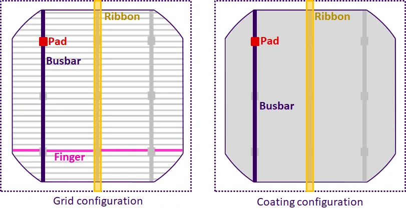
The Grid electrode represents the standard H-bar design for a solar cell electrode. It is made up of a set of fingers arranged at right angles to a series of busbars. Both fingers and busbars run the full extent of the substrate (i.e. to the edge of the wafer). This configuration would typically be used for the front electrode of a standard or PERC solar cell and for the front and rear electrodes of bifacial cells. Note that SunSolve allows the user to set the number of fingers to zero and/or the number of busbars to zero, effectively removing those elements from the grid design.
The Coating electrode represents a surface covered entirely by an electrode. It is made up of a series of busbars with a continuous layer of metal between each one. This configuration would typically be used to simulate the rear side of a standard screen print or the older style of PERC solar cell. Note that the coatings are applied all the way to the edge of the wafer and it is not possible to define a gap at the edge.
All configurations allow the definition of cell interconnection ribbons (sometimes called ‘tabbing’). Ribbons are aligned to the same axis as the busbars. The length of the ribbon is the same as the extent of the unit cell (i.e. the wafer size + any surrounding area). Ribbons can be applied to both the front and rear of the solar cell. In regular solar cells, there is typically one ribbon directly above each busbar, so the ribbons and busbars are spatially aligned, but in SunSolve it is possible to have any number of busbars or ribbons.
Note that the electrodes also contain pads (e.g. solder points between ribbons and busbars) as described in the grid calculator. The inputs to the pads affect the electrical calculation (i.e., the grid resistance) but they do not affect the optical calculations. As far as the optics is concerned, the pads are the same width and material as the busbars.
Interdigitated unit-grid definition
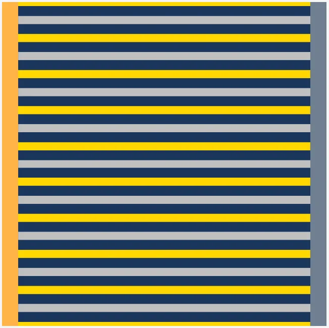
Section titled “Interdigitated unit-grid definition”This electrode pattern is based on the classical all back-contact solar cell design that was introduced in the early stages of the development of this technology (which typically had a single busbar for each contact). It is equivalent to the interdigitated pattern implemented in the original grid calculator.
Busbars are positioned at the very edge of the cell and, when there is more than one per electrode, are then evenly spaced across the wafer. Each busbar has a set of fingers that extend the full distance towards the busbar of the opposite electrode (they are interdigitated but do not make electrical contact). The fingers belong to either the outer electrode (which has the first and last finger at the cell edges) or the inner electrode. The outer electrode always has one more finger than the inner electrode.
The image below shows an example of the interdigitated unit-grid definition for the case of one busbar, ten outer fingers and nine inner fingers. The outer electrode is shown in yellow and the inner electrode in grey.
Busbar definition
Section titled “Busbar definition”The unit grid contains two busbars: one for the outer electrode and one for the inner electrode. These busbars lie at the boundaries of the unit grid.
When a cell has multiple unit grids, this increases the number of busbars but does not change the number of fingers per busbar.
Across the rear surface, busbars alternate between the inner and outer electrodes, so the pattern is always Inner → Outer → Inner → Outer, and so on. When multiple busbars are defined, the unit grid (as shown in the single busbar case) is repeated.
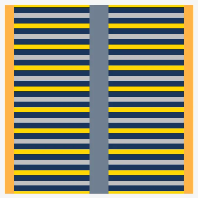
Example: 2 unit grids
Section titled “Example: 2 unit grids”The image below shows a cell with two unit grids (i.e. two busbars). Consequently:
- the outer electrode (yellow) has two busbars, located at the edges of the cell, and
- the inner electrode (grey) also has two busbars, which are adjacent in the middle of the cell and therefore appear as a single busbar with twice the width.
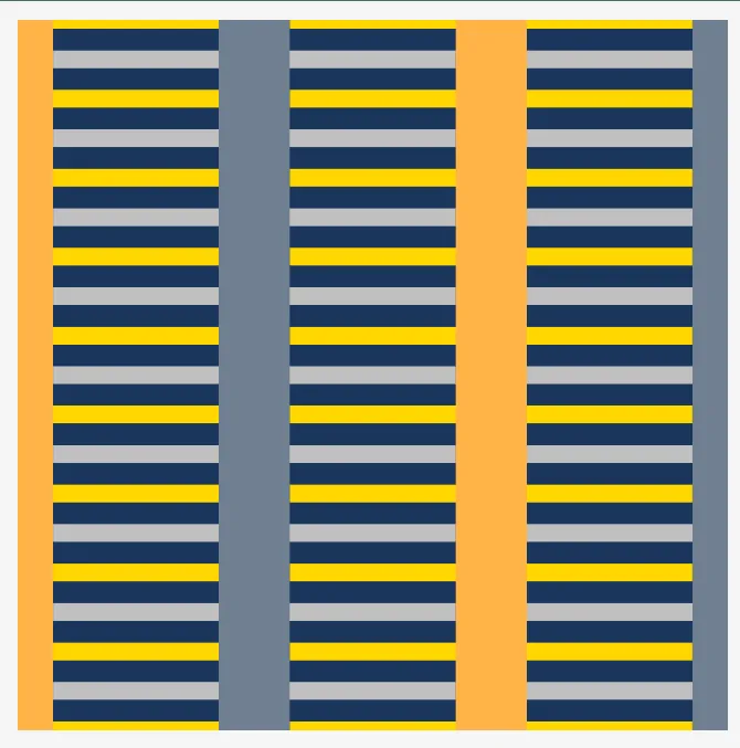
Example: 3 unit grids
Section titled “Example: 3 unit grids”The image below shows a cell with three unit grids (i.e. three busbars). Consequently:
- the outer electrode (yellow) has three busbars, with two of them adjacent so that the pattern appears as one regular-thickness busbar at the edge and one double-thickness busbar closer to the centre, and
- the inner electrode (grey) also has three busbars arranged so that the overall inner → outer → inner → outer pattern is preserved across the cell.
To emphasise the definition: “inner” and “outer” refer to the finger pattern, not the busbar pattern. The outer fingers of the outer electrode are located at the edges of the cell, which is why the outer electrode always has one more finger than the inner electrode.
Ribbon definition
Section titled “Ribbon definition”Interconnection ribbons can optionally be applied to the interdigitated unit-grid electrodes. When ribbons are enabled, they are positioned at the boundaries of the unit grids — the same positions where the busbars are located.
For a cell with unit grids, the total number of ribbon positions across the cell is (one at each boundary of the unit grids). At each position, the ribbon belongs to whichever electrode has a busbar at that location. Consequently the outer electrode and the inner electrode each have ribbons.
Like busbars, ribbons at the cell edges have width and ribbons through the middle of the cell, where two unit grids meet, have width .
Ribbons share the same orientation as the busbars and run the full extent of the unit cell (i.e. the wafer height plus any inter-cell spacing). The ribbon width and height are independent of the busbar dimensions and are defined separately by the user. The same ribbon definition is applied to both the inner and outer electrodes.
Finger, busbar and ribbon width definition
Section titled “Finger, busbar and ribbon width definition”The busbar width defines the width of each busbar within a unit grid. Busbars at the cell edges have width and busbars through the middle of the cell, where the unit grid is reflected, have width .
Similarly, the ribbon width defines the width of each ribbon within a unit grid. Ribbons at the cell edges have width and ribbons through the middle of the cell have width . The ribbon width is independent of the busbar width.
The finger width defines the width of the fingers in the middle of the cell. The outer fingers at the cell edges have half this width.
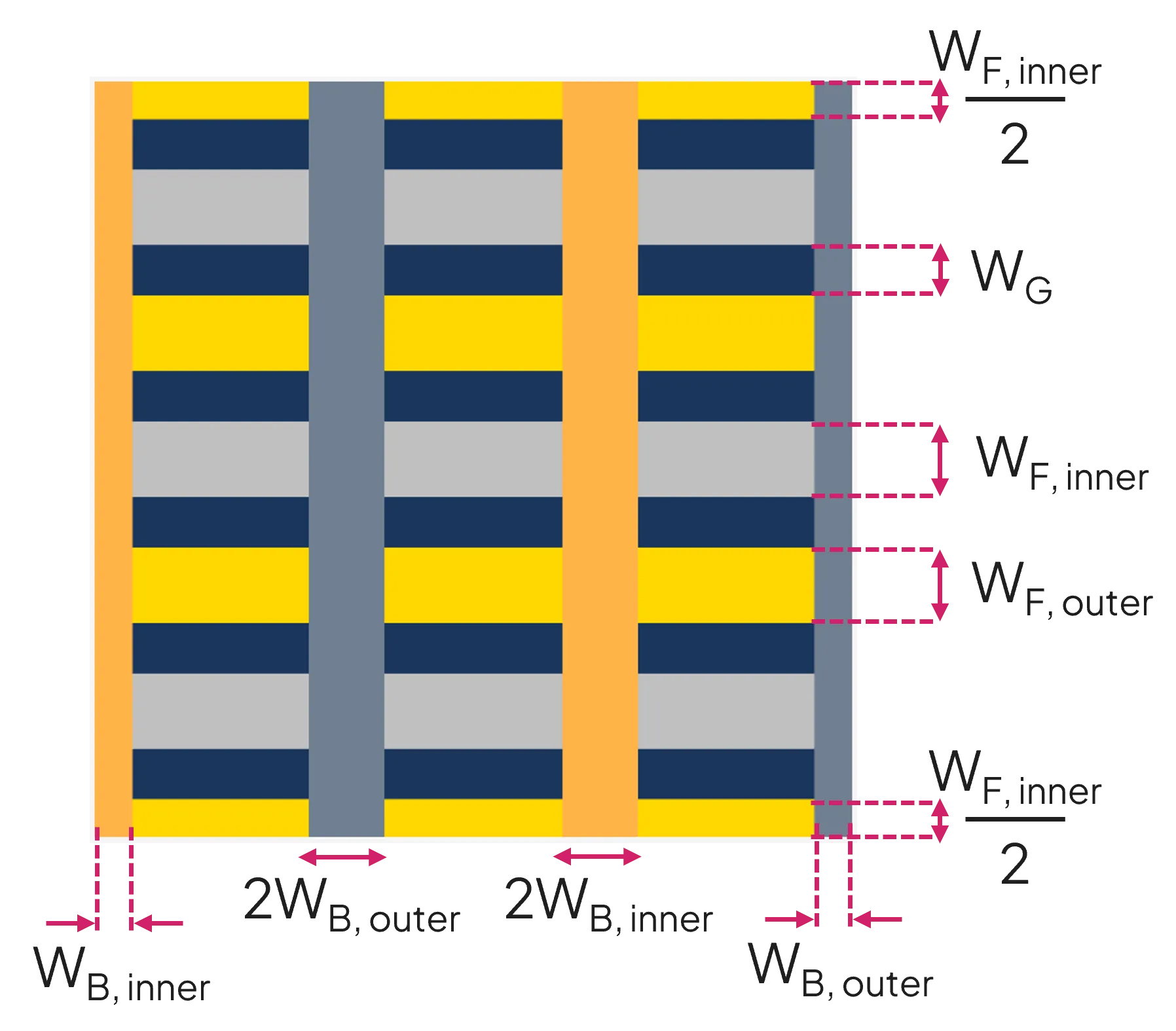
The user can define different finger widths for the inner and outer electrodes.
As shown in the figure, the fingers are laid out such that the cell edge passes along the central axis of the outer fingers. Equivalently, the outer fingers at the edge of the cell have half the nominal finger width.
The total finger width within a unit grid is
where:
- is the number of inner fingers,
- is the inner finger width, and
- is the outer finger width.
A common finger gap width is maintained. The gap width shown in the user interface is calculated as
where is the cell width.
In the optical model, there is no gap between a finger and the busbar it feeds; the metal is treated as a continuous region. Electrically, however, fingers from one electrode still terminate with a gap before the busbar of the opposite electrode, so the two electrodes remain isolated. The omission of these small gaps in the optical geometry simplifies the ray tracing without changing the way the electrical resistance of the grid is calculated.
Cross-sections of the grid elements
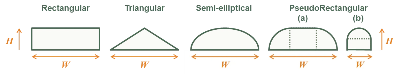
Section titled “Cross-sections of the grid elements”Several cross-sectional profiles are permitted for the fingers. Their dimensions are defined in the figure below. The “PseudoRectangular” cross section (labelled as a rounded rectangle in the user interface) is recommended for simulations of typical screen-printed fingers. It is defined as two quarter-circles and a rectangle, and it has two variants: (a) wide, when , and (b) narrow, when . It is semicircular when .
SunSolve forces the cross-sectional profile of busbars to be rectangular.
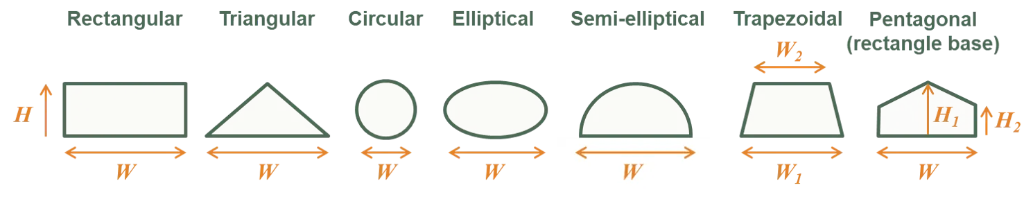
Eight cross-sectional profiles are permitted for the ribbons. The dimensions of seven of those are defined in the figure below. The rectangular ribbons can be textured, where the texture is on the side facing away from the solar cell.
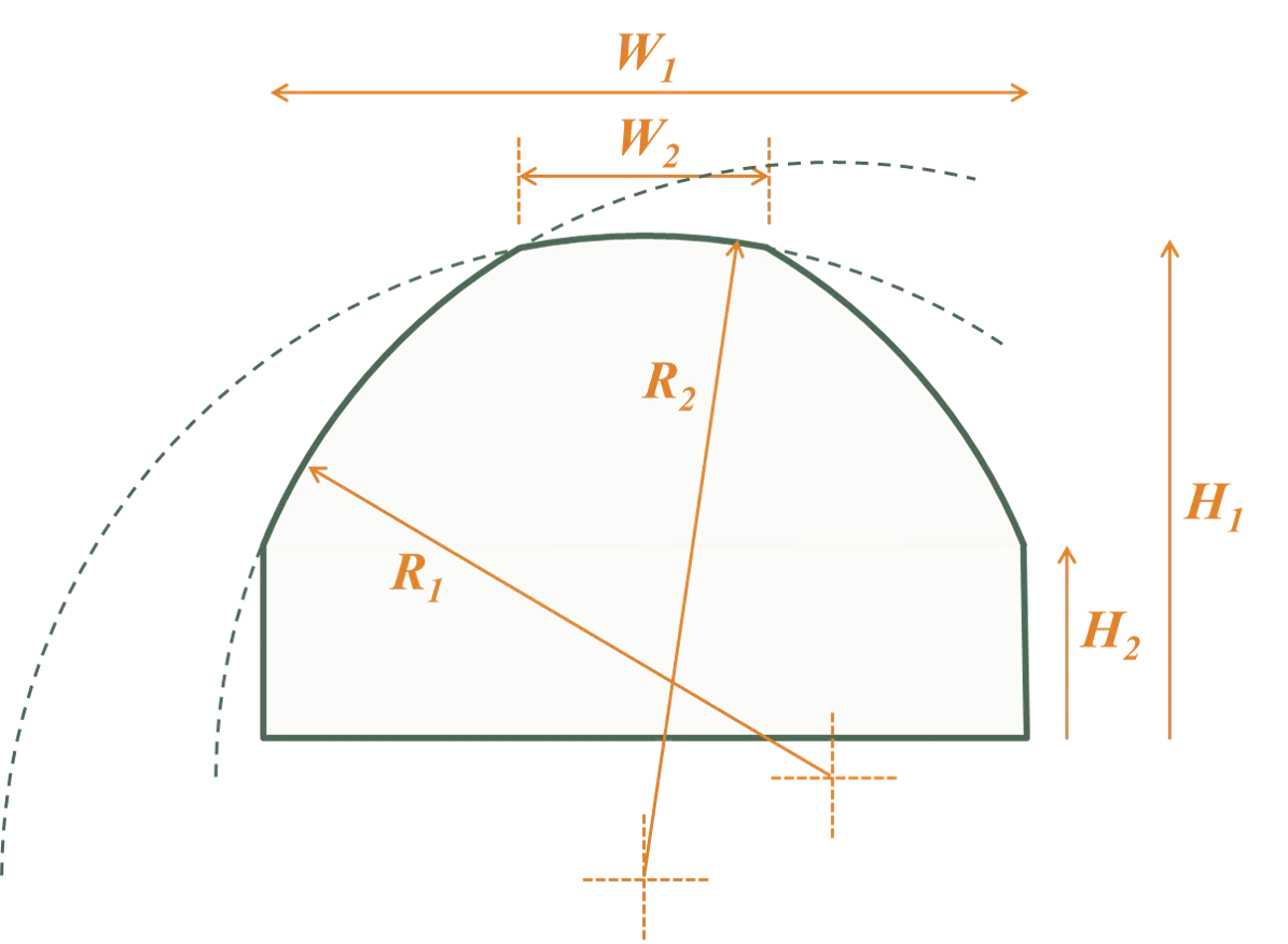
The final cross-sectional profile permitted for ribbons is called a “triple-arc” profile. It is defined by six inputs and hence requires a larger image:
These images are oriented such that the solar cell surface is at the bottom of each diagram, so they appear upside-down when visualising rear electrodes. For rear electrodes, the geometries are mirrored, but the side facing the solar cell remains the same; for example, the flat side of the semi-elliptical ribbons always faces the solar cell.
Contacts
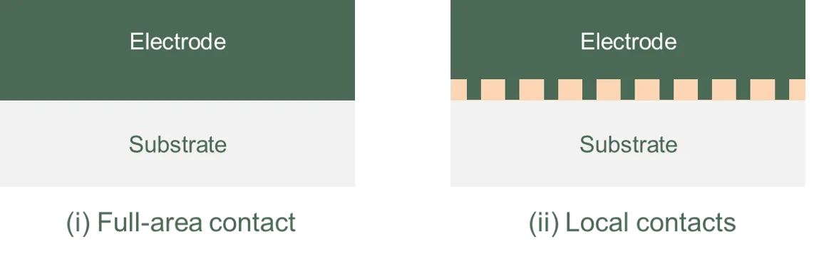
Section titled “Contacts”The contacts of a solar cell constitute the regions where the electrodes make electrical connection to the substrate.
In some cells, like conventional screen-printed solar cells, the contact represents the entire interface between an electrode and the substrate (a full-area contact); in others, like PERC solar cells, the contact only occurs at certain locations under the electrode (local contacts).
The figures below show example cross-sections of an electrode with (i) a full-area contact and (ii) local contacts.
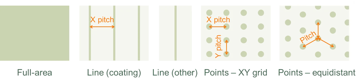
SunSolve permits several contact patterns. A contact pattern can be a ‘full-area’ pattern or it can be composed of lines or points.
When a line pattern is selected, it represents periodic lines for coatings but a single central line for fingers or busbars. When a point pattern is selected, the points can be either circular or rectangular, and they can be laid in either an XY grid or an equidistant pattern. The figures below illustrate the various contact patterns.
In SunSolve, the contact patterns affect the optical behaviour of the solar cell but not the electrical resistance of the metal electrodes. To account for current crowding at the contacts, increase the value of the series resistance accordingly.
Optical properties
Section titled “Optical properties”The optical properties of the electrodes and their interfaces can be defined for each individual element (finger, busbar, coating). These properties affect the ray tracing but have no impact on the resistance calculations.
The optical inputs for the contacts can be found by either clicking on the front or rear surface of the solar cell on the “Layers” tab, or by clicking on “Define front/rear electrode” on the “Electrodes” tab.
Optical material The optical material sets the refractive index, and , of the electrode element. This material can be selected from a library of materials whose and have been published, or customised values of and can be uploaded.
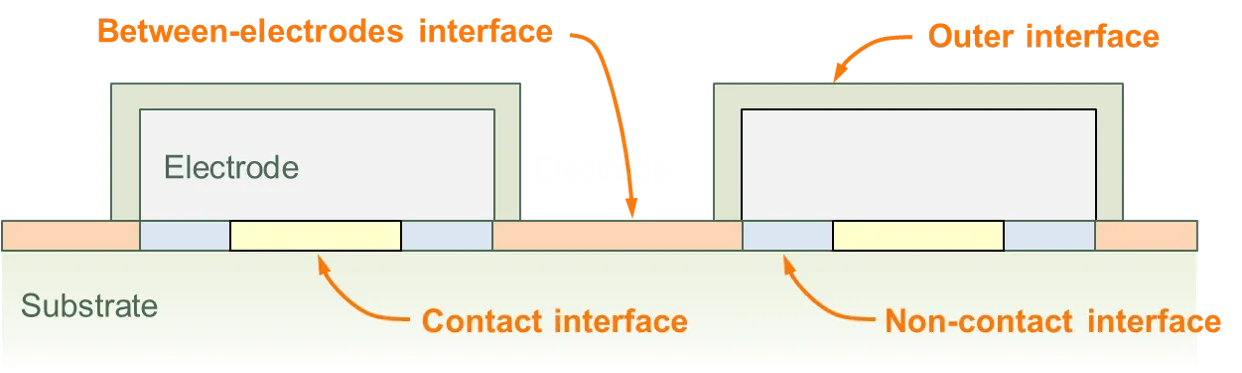
Electrode interfaces The optical properties of each electrode element (finger, busbar, coating) are also defined. There are either two or three interfaces:
- an outer interface, which faces away from the substrate of the solar cell,
- a contact interface, which defines the contact region between the electrode and the cell, and
- a non-contact interface, which defines the regions between the electrode and the substrate that are not in electrical contact (irrelevant for full-area contact patterns).
For finger and busbar electrodes (but not coating electrodes), the user also defines the substrate’s interface that lies between the electrodes.
The figure below illustrates the various interfaces associated with a substrate surface and electrode.
For each interface, the user defines:
- scattering properties, and
- either the reflectance, absorptance and transmittance (RAT) at the interface, or the optical properties of the element’s material and thin-film stack (with SunSolve then calculating the RAT using Fresnel and thin-film equations).
The interfaces for ribbons are defined similarly except that (i) the surface facing away from the cell can be textured, and (ii) the same interface is applied to all sides of the ribbon.
Here are two examples of how the electrode and substrate interfaces might be assigned to represent common solar cells.
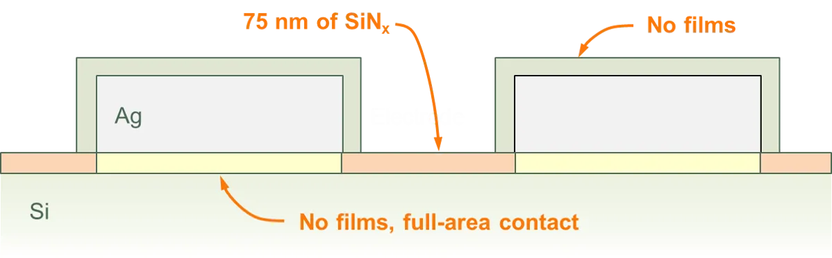
Example 1: Front-surface of a screen-printed solar cell
The front surface might be defined as having a grid of Ag, where there are no films under the electrodes but where SiNₓ lies between the fingers. Although it is not shown, the surface of the substrate would normally be textured with upright pyramids.
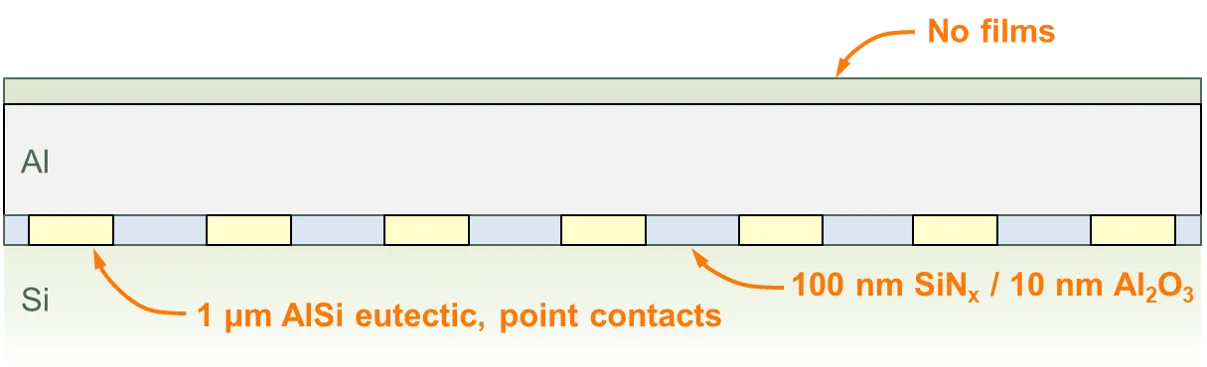
Example 2: Rear-surface of a PERC solar cell
The rear surface might be defined as having a coating of Al, where the Al is separated from the substrate by a film stack of SiNₓ on Al₂O₃ except at the point contacts where the interface is comprised of a thin film of AlSi eutectic.
Electrical properties
Section titled “Electrical properties”For each element the user can also define the electrical properties, including the metal resistivity and the electrode resistivity. These values are only used in the calculation of the grid electrical resistance and have no impact on the optical performance.