Optical layers
This section describes the optical layers in SunSolve Power.
Slabs and films
Section titled “Slabs and films”There are two types of layers: slabs and films.
A slab is a thick optically incoherent layer. The interaction of light with the slab is computed by geometric ray tracing and Beer’s law.
A film is a thin optically coherent layer that is conformal to the morphology of a slab. The interaction of light with a film, or a stack of thin films, is computed by the 1D thin-film matrix method.
By default, the thickness of a slab is restricted to the range 1–10⁵ μm and the thickness of a film is restricted to the range 0.001–1 μm. Write to support@pvlighthouse.com.au if you would like those restrictions modified.
Slabs can be added or removed from a module on the Layers tab. Each slab has
- a material, whose complex refractive indices can be found in the Refractive Index Library; and
- a bulk thickness.
The interface between two slabs is defined by
- a texture morphology, where the height of the texture is not included in the bulk thickness;
- an optical scattering model;
- and either
- a stack of thin films, where each film has its own material and thickness; or
- a ‘reflector’ with a defined reflectance, absorbance and transmittance.
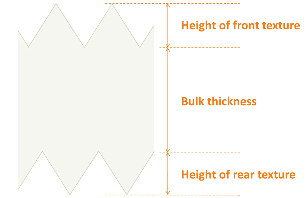
The image below shows how the total thickness of a slab depends on the user’s inputs for the bulk thickness and the height of the surface texture.
Films can be added or removed at any interface between slabs, where each film has
- a material, whose complex refractive indices can be found in the Refractive Index Library; and
- a thickness.
The thickness of the films is used to calculate the optical behaviour of the interface, and, if requested, the generation profile within the film. The thickness of the films do not, however, contribute to the thickness of the module, which is computed only from the thickness of the slabs and their morphology.
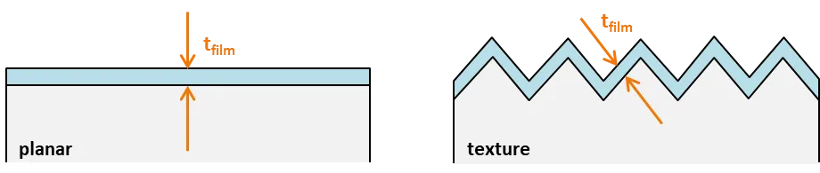
The film thickness represents the dimension shown in the image below. It defines the thickness of the film in the direction perpendicular to the underlying plane. Thus, films are assumed to be perfectly conformal to texture.
The film thickness can be constant or variable. If it is variable, then the film thickness is recalculated every time a ray interacts with the interface. In such case, one of two probability functions can be applied: (a) top-hat or (b) Gaussian. Examples of these functions are plotted below in the left graph. If a Gaussian distribution is selected, then upper and lower limits to the thickness are applied; the limits can be no greater than 4 standard deviations from the mean, and the lower limit cannot be less than zero.
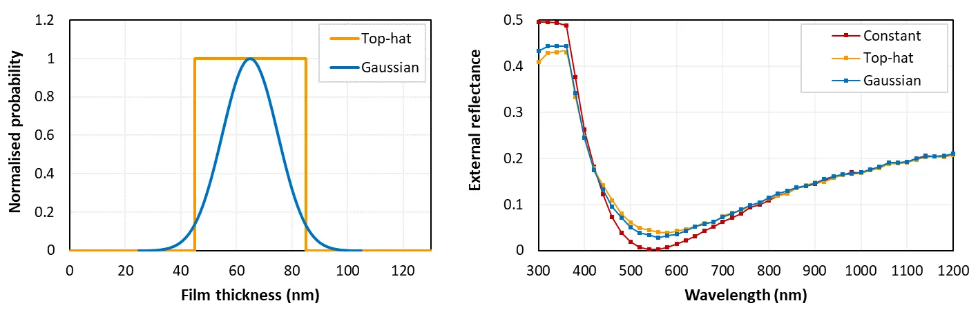
The figure above gives an example of how the different options for film thickness can affect the results. The right graph plots the external reflection for planar silicon coated by an SiNₓ film of three thicknesses: (i) constant 65 nm, (ii) a top-hat function of 65 ± 20 nm, and (iii) a Gaussian function with a mean of 65 nm, a standard deviation of 10 nm, and lower and upper limits of 25 and 105 nm. These functions are plotted in the left graph.
By default, SunSolve assumes that all films have a constant thickness. To set an interface with films of variable thickness, navigate to the Options tab, check ‘Enable variable ’ and select the desired interfaces. The selected interfaces will then contain the additional inputs that are required to define films of variable thickness.
Material properties
Section titled “Material properties”SunSolve computes the optical behaviour of light rays as they pass through materials and as they interact with the interface between materials. These calculations require knowledge of each material’s wavelength-dependent complex refractive index: and .
Materials can either be selected from our pre-loaded dataset or from your own datasets. There is a video that explains how to upload datasets, and all and data can be plotted and downloaded in our Refractive Index Library.
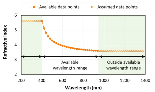
To determine and at some desired wavelength , SunSolve linearly interpolates the refractive-index datasets. If is shorter than the shortest available wavelength in a dataset, SunSolve assumes that and equals and at the shortest available wavelength. An equivalent assumption is applied for long wavelengths. The graph below illustrates this approach.
Collecting layers and light-generated current
Section titled “Collecting layers and light-generated current”A ‘collecting’ layer contributes towards the electrical current produced by the module. That is, some fraction of the photons absorbed by a collecting layer are converted into free carriers and ‘collected’, thereby contributing to the light-generated current of the solar cell.
In most of the SunSolve templates, the main slab is the only collecting layer. Like a conventional module with c-Si solar cells, only the silicon slab generates current.
It is possible, however, to set other layers as being collecting. For example, the film on the front side of the solar cell can be collecting, like the a-Si film in a heterojunction solar cell, or the perovskite layer of a perovskite–Si tandem solar cell.
Although any film can be collecting, SunSolve only permits one collecting slab.
All collecting layers contribute towards the same light-generated current :
where represents each collecting layer and
where is the incident photon current as determined from the inputs on the Illumination tab, is the fraction of the incident light that is absorbed by the band-to-band process within the collecting layer as determined by the ray tracing, and is the collection efficiency of the collecting layer.
This calculated value of is used by the electrical solver to calculate the current–voltage curve and maximum-power produced by the simulated cell or module.
Layers can be assigned as ‘collecting’ on the Circuit tab in the ‘Collection efficiency’ section. Once a layer is assigned as collecting, its collection efficiency can be set to be either constant or variable with wavelength.
Layer absorption
Section titled “Layer absorption”There are two types of optical absorption in a semiconductor: band-to-band absorption (BBA) and free-carrier absorption (FCA).
When light is absorbed by a BBA process, it means that an electron within the valence band received sufficient energy to be transferred into the conductance band. The newly excited electron becomes a ‘free carrier’ and it contributes to the light-generated current. (It also means that a hole is transferred from the conductance to the valence band, and it too becomes a free carrier.)
When light is absorbed by an FCA process, the energy of the photon is absorbed by either an electron that is already in the conduction band or a hole that is already in the valence band. Although this process transfers a free carrier to a higher energy state, it quickly loses that energy (as heat) and the carrier returns to its original state. Unlike BBA, FCA does not contribute to the light-generated current.
In SunSolve, it is possible to compute both sources of absorption.
By default, SunSolve assumes the imaginary component of a collecting material’s refractive index represents BBA. When this is the case, all of this absorption contributes to the generation current. (The imaginary component , commonly referred to as the extinction coefficient, relates to the absorption coefficient by the equation .)
It is, however, possible to calculate both FCA and BBA. To do so, check ‘Include FCA’ on the Options tab, and select which collecting layers have FCA within the FCA panel.
For each layer assigned with FCA, the user must first define what is meant by the values of in its material dataset. Remember, the materials are selected on the Layers tab, and their refractive-index datasets, i.e., and , can be downloaded from our Refractive Index Library.
Specifically, the checkbox under ‘Optn’ in the FCA table gives the user the option to define the material’s as including or excluding FCA. When unchecked, and when checked, . For example, the published data for in Si almost always excludes FCA, in which case , and the input should be unchecked. In other materials, might be derived from measurements of a material’s total absorption, in which case would include both BBA and FCA and the input should be checked.
Next, the user assigns an FCA model to each layer. There are two types of models:
- A published model, whereby the user enters the concentration of free electrons and free holes and SunSolve computes by the equations described in our FCA calculator. These FCA models are described in more details in the next section below.
- A custom model, whereby equals in a user-selected material. When applying this option, a user would normally select a custom material whose values were specifically set to the desired .
With these inputs, the user has assigned certain layers as having two extinction coefficients: and , where the combined extinction coefficient is simply .
SunSolve then solves the ray tracing using for all layers to determine the total absorptance in each layer . Following the ray tracing, the fraction of that absorption attributed to BBA and FCA is and , respectively. (We have not found a citation for this assumption.)
We thank Hanwha Q cells for co-funding the upgrade to include free-carrier absorption.
Free-carrier absorption models
Section titled “Free-carrier absorption models”FCA in crystalline Si
Section titled “FCA in crystalline Si”SunSolve provides several models to calculate FCA of c-Si from the free-carrier concentration, most of which assume a temperature of 300 K.
- Classical Drude model: Equation in Smith (1959), and Schroder (1978) (Eq 1), and in Isenberg (2004) (Eq 1, where second factor is unity).
- Schroder (1978): Equations 5 and 6 in Schroder (1978). Fit to data for λ > 4000 nm and dopant concentrations of 10¹⁶ to 10¹⁹ cm⁻³ in c-Si.
- Green (1995): Equation 4.8 in Green (1995). Derived for λ > 2500 nm and carrier densities ~10¹⁸ cm⁻³ in c-Si.
- Isenberg (2004): Equation 4 with parameters from Table I in Isenberg (2004). Limited to 1200 nm in c-Si.
- Rudiger (2013): Rudiger (2013). Derived from a fit to experimental data over the range 1200 nm < λ < 2000 nm in diffused c-Si and carrier concentrations between 10¹⁷ and 10²⁰ cm⁻³.
- Xu (2013): Xu (2013). Derived from a fit to experimental data over the range 1000 nm < λ < 1200 nm in diffused c-Si and carrier concentrations between 10¹⁷ and 10²⁰ cm⁻³.
- Baker-Finch (2014): Baker-Finch (2014). Derived from a fit to experimental data over the range 1000 nm < λ < 1500 nm in diffused c-Si and dopant concentrations between 10¹⁸ and 3 × 10²⁰ cm⁻³.
- Baker-Finch LL (2014): Baker-Finch (2014). Lower limit to the parameterisation of best-fit.
- Baker-Finch UL (2014): Baker-Finch (2014). Upper limit to the parameterisation of best-fit.
The first model for FCA is derived from the classical ‘Drude’ treatment of the random collisions of free carriers in a solid. It is common for the approach of Smith (1959) to be applied (e.g., in Schroder (1978), Horwitz (1980), Isenberg (2004), Rudiger (2013)), where in this embodiment, has a linear dependence on free carrier concentration and a parabolic dependence on wavelength. The user must also enter the mobility of free carriers. We apply Eq. 1 of Schroder (1978). The remaining models are parameterisations for c-Si at 300 K.
FCA in any material
Section titled “FCA in any material”SunSolve also includes a ‘generic parameterisation’ model:
where , , and are constants, and are the electron and hole concentrations in cm⁻³, and is in nm. This equation is the general form of all of the above models except the Drude and Isenberg models.
The generic parameterisation is also used by PC1D. The PC1D help file contains inputs for c-Si and a few n-type semiconductors from old sources (1967, 1978, 1981); find them by navigating within PC1D help via ‘device menu’ → ‘region parameters’ → ‘material’.
FCA recommendation
Section titled “FCA recommendation”For crystalline silicon (including polycrystalline silicon) at 300 K it is recommended to use the Baker-Finch model (2014). For other materials and temperatures it is recommended to use custom FCA data derived from experimental measurements, or the generic parameterisation if representative inputs are available.