Module electrical layout
The electrical layout defines how cells within a module are wired together. This includes the circuit topology (how strings of cells are connected), connector row configuration, bypass diode configuration, and any additional resistive components. These inputs are found in the Circuit tab of the module popover, which appears when you load or preview a module.
The electrical layout is shared between both simple and complex module types. The physical cell arrangement (dimensions, spacing, and cell groups) is configured in the Layout tab and described on the module cell layout page. The inter-cell spacing from the layout inputs also affects the calculated ribbon length used in the series resistance calculation.
For the underlying theory of the module circuit model, see Module electronics.
Circuit type
Section titled “Circuit type”The circuit type determines the fundamental wiring topology used to connect cells within the module. The following options are available:
-
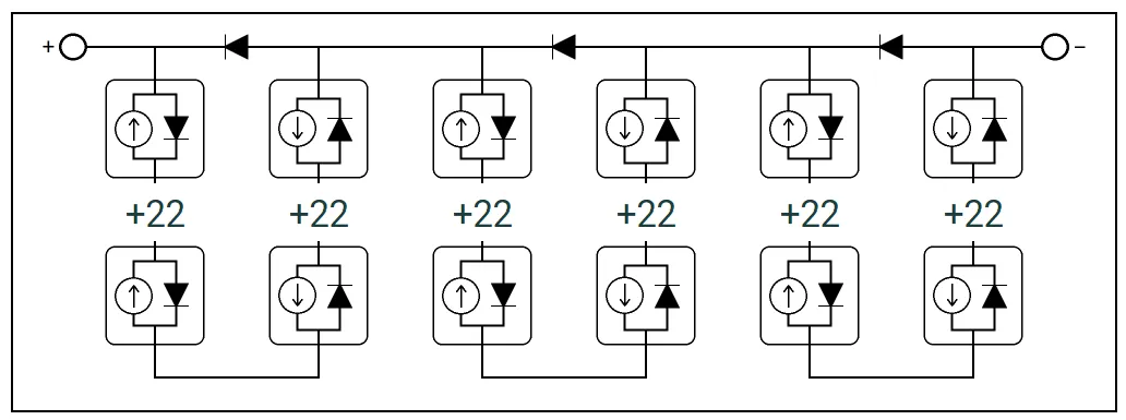
Vertical strings — the standard layout for crystalline silicon modules. Cells are arranged in columns, with each column divided into substrings of series connected cells. Connector rows separate the substrings and define the bypass diode protection zones. This is the default and most commonly used option.
-
Horizontal strings — a layout where cells are connected in series within horizontal strings, with multiple strings connected in parallel. This is commonly used for thin-film modules.
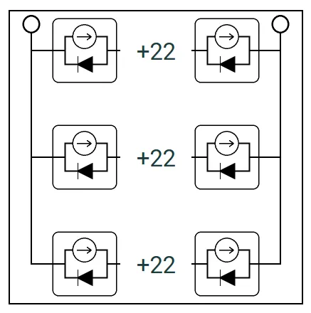
Left: Vertical strings — cells are wired in series within vertical columns. Right: Horizontal strings — cells are wired in series within horizontal rows.
Connector rows
Section titled “Connector rows”For the vertical strings circuit type, the connector rows input is shown. This defines the number of horizontal connector rows in the circuit, which determines how the column of cells is divided into substrings.
A module with connector rows has substrings per column.
For example, the figures below show two common configurations for a 6-column module. On the left, the layout has 2 connector rows with a single substring of cells in each column. On the right, there are 3 connector rows, dividing each column into 2 substrings.
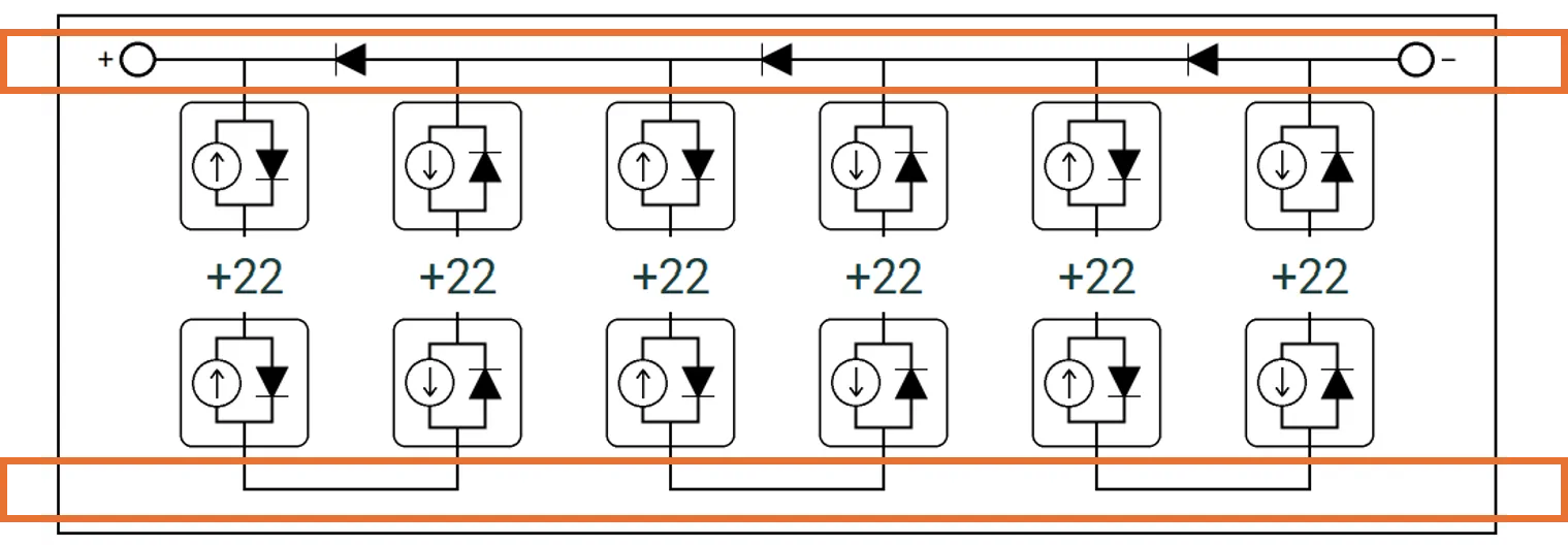
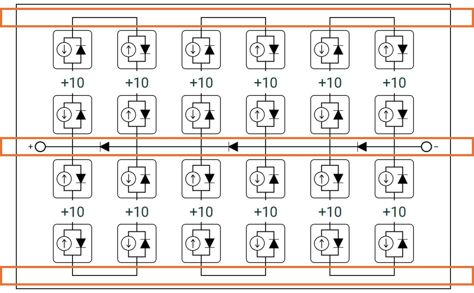
Left: 2 connector rows (highlighted in orange) — each column has 1 substring. Right: 3 connector rows (highlighted in orange) — each column is divided into 2 substrings, with a bypass diode protecting each substring.
The value is adjusted using increment/decrement buttons. The minimum value is 2 (no split). The maximum value is the rows of cells in the module + 1.
Circuit diagram
Section titled “Circuit diagram”For the vertical strings layout, an interactive circuit diagram is displayed showing the wiring topology of the module. The diagram shows:
- Cell strings — vertical columns of cells with arrows indicating current flow direction (up or down)
- Connectors — the wiring elements between strings, shown as bypass diodes, resistors, open circuits, or terminals
Editing the circuit
Section titled “Editing the circuit”The circuit diagram is interactive. Different elements respond to clicks as follows:
Internal connectors — clicking an interior connector selects it, highlighted with an orange border. An editor panel appears below the circuit diagram with a Type dropdown offering the following options:
- Bypass diode ← / Bypass diode → — the connector acts as a bypass diode, using the same model parameters configured in the bypass diodes section. The arrow indicates the current flow direction under forward bias.
- Open circuit — the connector is electrically disconnected.
- Resistor — the connector acts as a purely resistive connection. The Resistance input is fixed to a value of 0 Ω reflecting a short-circuit condition.
Clicking the selected connector again deselects it and hides the editor panel.
Cell strings can be clicked to toggle current flow direction.
Terminal connectors (leftmost and rightmost columns) control the positive and negative connection points of the module circuit. The positive terminal appears in the first column and the negative terminal appears in the last column of the connector grid. To reposition a terminal, click on a different connector in the same column — the terminal moves to the clicked position and the previous location is reset to an open circuit. There is always exactly one positive terminal and one negative terminal in the circuit.
Show full circuit
Section titled “Show full circuit”When a module has many cells per substring, the circuit diagram displays a compressed view by default. Checking Show full circuit expands the diagram to show every cell individually. This may not render well for very large cell counts.
Adding and removing columns
Section titled “Adding and removing columns”For the vertical strings layout, short-circuit columns can be inserted or removed from the circuit:
- Check Add columns to display ”+” buttons at insertion points between existing columns
- Check Remove columns to display ”−” buttons on existing short-circuit columns
These short-circuit columns represent additional current paths in the circuit (e.g., for modelling interconnection busbars or alternative wiring schemes).
Clicking on a string element in an added column selects it, highlighted with an orange border. The String component editor panel appears below the circuit diagram with a Type dropdown offering the following options:
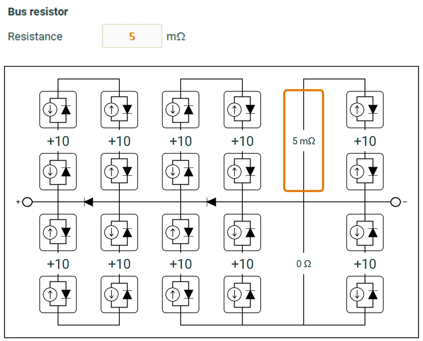
- Bus resistor — the string acts as a purely resistive connection. A Resistance input sets the ohmic resistance value. A resistance of 0 Ω represents a perfect short circuit (ideal bus bar). This is the default for new columns.
- Bypass diode ▲ (up) / Bypass diode ▼ (down) — the string acts as a bypass diode with an associated series resistance. The diode uses the same model parameters configured in the bypass diodes section. A Series resistance input is shown to set the resistance in series with the diode.
- Open circuit — the string is electrically disconnected.
Clicking the selected string again deselects it and hides the editor panel.
A short-circuit column inserted between cell columns, with the string component editor shown for the selected string.
Bypass diodes
Section titled “Bypass diodes”Each substring in the module is protected by a bypass diode. The bypass diode model can be configured as either Simple or SPICE level 1. See the bypass diode model technical reference for the full equations.
Simple model
Section titled “Simple model”The simple bypass diode model uses two parameters:
SPICE level 1 model
Section titled “SPICE level 1 model”The SPICE level 1 model provides additional parameters for more accurate diode characterisation:
Exporting bypass diode IV curves
Section titled “Exporting bypass diode IV curves”Click → get bypass diode IV(T) to compute and export the bypass diode IV curve at multiple temperatures as a CSV file. This includes both forward and reverse bias characteristics.